July 20, 2006 feature
Nanoparticles self-assemble through chemical lithography

Nanoparticles – while possessing some amazing properties of strength and power – are also delicate little things, when it comes to manipulating them for use in nanodevices. Many scientists consider that the most promising method of incorporating nanoparticles into functional structures is through their own self-assembly, an approach commonly attempted through different lithography techniques.
Nanolithography, which involves making a periodic pattern of the nanometer-sized structures, requires absolute control of the size, shape, spatial distribution and functionality. Scientists can achieve such control using nanoparticles, which function as “quantum dots” or artificial atoms, if they can be arranged in regular arrays, particle by particle.
Arranging these particles by hand and/or scanning microscope tips is technologically impractical due to the unfeasible amount of time it would take. Therefore, nano engineers manipulate the nanoparticles’ properties by various treatments so that they can simply “dump” the particles in a treated area, whereby they automatically arrange themselves. This ability is, in a sense, the basis of all nanotechnology.

One of the newest types of nanoparticle self-assembly – developed by scientists K. Prabhakaran and team from institutions in the U.S., Japan and Germany – is called “chemical lithography.” The process, the scientists demonstrate, can effectively form periodic arrays of very stable nanoparticles that don’t succumb to many of the defects and limitations of previous lithography techniques (which include, for example, atomic force microscope dip-pen lithography, laser lithography, electron beam lithography, embossing, etc.). Chemical lithography, instead, is a combination of techniques, where particle arrangement is controlled by differences in reactivity – a characteristic determined by exposing particles and surfaces to an assortment of chemical treatments.
“We believe that this approach can be universal and extendable to more specific functionalities,” wrote Prabhakaran, et al. in a recent issue of Nanotechnology. “This method has the potential to deliver tailored functional nanoarchitectures [which] will play a major role in realizing completely self-assembled nanodevices.”
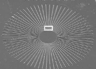
The scientists used luminescent yttrium aluminum garnet (YAG) nanoparticles assembled on a silicon wafer, synthesizing the particles through doping and crystallization to determine their shape and composition. Before placing the particles on silicon wafers, the scientists pre-patterned the wafers using etching techniques based on a phenomenon called “atomic step movement.” Because atom-high steps innately exist on silicon surfaces, the scientists could move these steps during high-temperature treatments to fabricate a desired pattern. Chemical reactions (between the silicon, nitrogen and oxygen) caused very thin nitride linings to form in accordance with the atomic step boundaries, thereby pre-patterning the wafers.
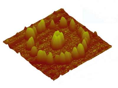
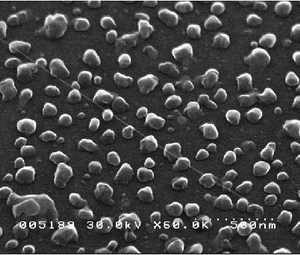
Then, in order to align the particles along the pattern on the wafer, the scientists annealed the samples in an ultra-high vacuum chamber for several hours. After being heated at temperatures ranging from 1000 to 1500 degrees Fahrenheit (500-850 degrees Celsius), the scientists not only unveiled precisely aligned particles (see figures), but also another advantage. Measuring the nanoparticles’ alignment after the annealing process revealed the strength of the particles using this technique. Generally, many nanoparticles suffer from photobleaching, which is damage caused after exposure to high intensity light; these particles, on the other hand, remained intact after prolonged illumination of the scientists’ fluorescent imaging measurements.

“For the sake of applications, it is important to have stability in the luminescence characteristics in the aligned form,” Prabhakaran told PhysOrg.com. “One of the problems associated with luminescent particles is that when they undergo photobleaching, the particles cease to emit light in a continuous manner. These systems are not very useful for real applications. In our method, however, one can envisage a nanoarchitecture which involves an assembly of particles which are sensitive to a wide range of external influences and can initiate a particular sequence of events.”
Prabhakaran explained that it is possible to achieve precise “nanoarchitecturing” involving many sorts of applications with the ability to assemble particles that have a particular wavelength or magnetic property by selectively activating or sensing such properties.
“The message that this work gives is that it is possible to generate species of the same element, which behave differently or exhibit different chemical reactivity, depending on their spatial location,” Prabhakaran said. “This way, one can have different functional structures by performing selective chemical reactions. The importance of self-assembly in nanotechnology is further emphasized by the fact that the nanostructures are prone to destruction by the conventional methods in semiconductor processing. For example, if we are to employ the quantum dots for applications, we should be able to interconnect them so that they can communicate to each other.”
Citation: Prabhakaran, K., Gotzinger, S., Shafi, K. V. P. M., Mazzei, A., Schietinger, S., and Benson, O. ”Ultrafine luminescent structures through nanoparticle self-assembly.” Nanotechnology 17 (2006) 3802-3805.
By Lisa Zyga, Copyright 2006 PhysOrg.com


