This article has been reviewed according to Science X's editorial process and policies. Editors have highlighted the following attributes while ensuring the content's credibility:
fact-checked
proofread
Advancing transistor technology with triply-degenerate semimetal PtBi₂

Despite its promising characteristics in condensed matter physics, the triply-degenerate semimetal PtBi2 has been largely unexplored in practical applications, particularly in semiconductor technology. The main difficulties include a lack of empirical data on the integration of PtBi2 with existing semiconductor components and the need for innovative approaches to leverage its unique properties, such as high stability and mobility, within the constraints of current electronic manufacturing processes.
Addressing these challenges could unlock new possibilities in transistor design and broader semiconductor applications, making it crucial to explore the practical applicability of PtBi2 in real-world electronics.
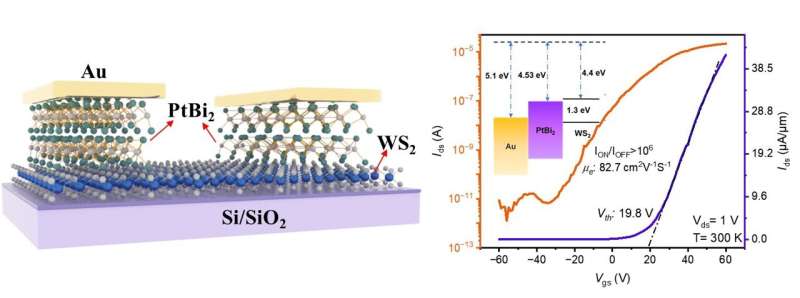
A research team from Songshan Lake Materials laboratory successfully used PtBi2 flakes as interlayer contact between metal electrodes (Au) and WS2, a widely studied semiconductor. This method significantly enhanced the transistor performance, achieving a switching ratio above 106 and an average mobility of 85 cm²V⁻¹s⁻¹, thus meeting and potentially exceeding the stringent demands of integrated circuit applications.
The work is published in the journal Materials Futures.
Future research is poised to explore diverse PtBi2-based device architectures, focusing on optimizing the interplay between device miniaturization and enhanced performance. Given its promising electronic properties, application of PtBi2 could extend beyond traditional transistors to optoelectronic and spintronic devices.
"PtBi2 stands out due to its unique electronic structure, exceptional air stability and ability to facilitate van der Waals contacts, which simplifies the device fabrication process and leads to stable, long-term device performance," explained Prof. Lin, one of the lead researchers of the study.
"This material not only reduces the Schottky barrier, which is a common challenge in transistor technology but also avoids the Fermi pinning effect that occurs during metal deposition."
One of the most notable aspects of the study is the use of a non-destructive van der Waals transfer technique, which maintains the integrity of the materials and interfaces. The researchers believe this method will offer a novel path to integrate new materials into semiconductor technology.
The findings are expected to have broad implications for the semiconductor industry, providing a new material platform for developing more energy-efficient electronic devices with high functionality. The team is optimistic about the future applications of PtBi2, not only in transistors but also in optoelectronic and spintronic devices.
More information: Bohan Wei et al, Triply Degenerate Semimetal PtBi2 as van der Waals Contact interlayer in Two-Dimensional Transistor, Materials Futures (2024). DOI: 10.1088/2752-5724/ad47cf
Provided by Songshan Lake Materials Laboratory


