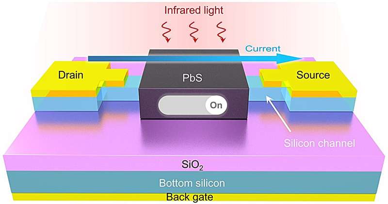
The schematic structure of the photo-FinFET, featuring a fin-shaped silicon channel for carrier transport, surrounded by a thin film of lead sulfide (PbS) acting as the infrared-sensitive gate. Credit: Opto-Electronic Science (2024). DOI: 10.29026/oes.2024.230046
Infrared detectors are the core components of infrared detection systems and play an important role in fields such as night vision, remote sensing, and health monitoring. In this context, the utilization of mature silicon technologies to develop miniaturized, highly integrated, and cost-effective infrared detectors becomes a key research direction.
However, the intrinsic large bandgap of silicon prevents it from detecting infrared light with wavelengths beyond 1100 nm, which poses obstacles to the development of silicon-based infrared detection technology.
To address this issue, an effective and promising strategy is to combine silicon with infrared-sensitive materials to construct hybrid photodetectors, thereby expanding the spectral response range of silicon-based devices. However, in existing designs of photodiodes and field-effect phototransistors, the traditional two-dimensional planar structure limits the transport efficiency of photocarrier and the modulation ability of photovoltage, thus affecting device performance.
Therefore, the exploration and design of novel device architectures to achieve broadband photoresponse and improve sensitivity are crucial for advancing silicon-based infrared detection technology.
Researchers now propose, in Opto-Electronic Science, a photo-driven fin field-effect transistor (photo-FinFET).
The design of photo-FinFET takes inspiration from the classical microelectronic device design, the FinFET, which extends photovoltage control from a two-dimensional plane to a three-dimensional space, thereby realizing silicon-based infrared detection with high sensitivity and broadband photoresponse.
The structural design of photo-FinFET offers two advantages: (i) it leverages the PbS-Si heterojunction to deplete the channel, suppressing the dark current. (ii) The photovoltage generated at the PbS-Si interface can efficiently modulate the channel, resulting in a substantial infrared photoresponse.
Experimental results demonstrate that the photo-FinFET achieves a broad spectral response from visible light (635 nm) to short-wave infrared (2,700 nm) at room temperature, with a fast response speed (150 μs). Additionally, the low dark current enables the photo-FinFET to exhibit equivalent noise powers of 3.2×10⁻¹² W·Hz-1/2 and 2.3×10⁻¹¹ W·Hz-1/2 under 1,550 nm and 2,700 nm illumination, respectively.
The design of the infrared fin gate enables the photo-FinFET to not only overcome the intrinsic light absorption limitation of silicon, but also exhibit low dark current and broadband infrared photoresponse at room temperature.
Moreover, the fabrication process of the prototype device is compatible with silicon-based CMOS technologies, providing promising methods for the development of low-cost, low-power, and high-sensitivity silicon-based infrared detectors.
More information: Jintao Fu et al, Photo-driven fin field-effect transistors, Opto-Electronic Science (2024). DOI: 10.29026/oes.2024.230046
Provided by Compuscript Ltd


