Credit: ACS Photonics (2024). DOI: 10.1021/acsphotonics.3c01532
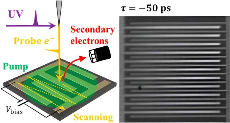
Researchers at University of Tsukuba have developed an ultrafast time-resolved scanning electron microscopy instrument by integrating a scanning electron microscope with a femtosecond laser. This innovative system facilitates the observation of the instantaneous states of various materials. Their paper is published in the journal ACS Photonics.
The rapid advancement of electronic devices, which underpins modern society, demands increasingly faster operating speeds. Active research and development efforts are directed toward the next generation of technologies that surpass today's fastest 5G band, known as Beyond 5G.
To facilitate the development of these ultrafast semiconductor devices, precise measurement of high-speed phenomena such as electric potential and electron transfer within the devices is crucial for understanding their operation.
To tackle this challenge, the research group combined a scanning electron microscope with a femtosecond (10−15 second) laser to measure potential changes in device materials with high temporal resolution.
They used this instrument for performing scanning electron microscopy (SEM) of a photoconductive antenna device on a GaAs substrate and obtained SEM images with a resolution of 43 picoseconds.
These findings enable the measurement of electrical circuit performance across a bandwidth of 23 GHz, which exceeds the frequencies typically used in 5G communications.
This breakthrough technology offers non-contact, high-speed, three-dimensional measurement of dynamic potential changes at arbitrary points within device structures. It is anticipated to be a vital tool in the development of next-generation electronic devices.
More information: Yusuke Arashida et al, Visualizing the Transient Response of Local Potentials on Photoconductive Antennas Using Scanning Ultrafast Electron Microscopy, ACS Photonics (2024). DOI: 10.1021/acsphotonics.3c01532
Journal information: ACS Photonics
Provided by University of Tsukuba


